This page serves as a repository for chip images I have traced and analyzed.
If you'd like to contact me, email quietust at either @qmtpro.com or @gmail.com. I can also be found on the NESdev Discord server, as well as in the #nesdev IRC channel on EFnet.
After further examining the RP2C02 surface die shots, I've managed to locate several additional important bits: the VRAM address register (including part of the logic that resets only the horizontal scroll bits at the end of each scanline), part of the background render pipeline (and the fine horizontal scroll register used to index into it), and what appear to be the pixel/scanline counters used during rendering. I'll update the "Regions" pseudo-layer image later today.
I've also received news that the person who normally does the chip depackaging/delayering/photography for Visual6502.org has been abnormally busy for the past several months and does not expect to have any free time until early next year, so in all likelihood there will be no further progress on the Visual 2C02 for quite a long time.
Since nothing's been happening with the RP2C02 for the past month and a half, I've started tracing my first non-NES chip: the Motorola 68000.
I've been gradually altering the ChipSim visualizer to work better with non-CPU chips, most notably replacing the "sample program" with a way to interact with I/O ports. It isn't complete yet, but hopefully it'll be ready by the time I've got enough data to simulate the RP2C02.
In other news, I've just discovered a missing transistor in the RP2A03's DPCM address counter, which caused A12 to always be set after the counter was incremented. Fortunately, the new chip tracing workflow I'm using for the RP2C02 should be immune to this sort of mistake.
In the process of tracing the RP2C02's metal layer and vias, I managed to determine the locations of a few specific bits of functionality. For example, a rather large block in the bottom-left contains 8 copies of a particular structure which contains an 8-bit counter and a pair of 8-bit shift registers, almost certainly responsible for sprite rendering.
What I've found so far has been added to the "Regions" pseudo-layer image - further information will likely not be feasible to collect until the chip is delayered, and that could take anywhere from weeks to months depending on the Visual6502 project's priorities (and I'm not in a position to ask that those priorities be changed in favor of the RP2C02).
Random trivia: the RP2C02G contains at least 26,955 vias (connections between Metal and Polysilicon/Diffusion) - factoring in copy/paste for repetitive regions (such as Sprite and Palette RAM), tracing them out involved about 1 left-click every 2 seconds over the course of about 16 hours. Not surprisingly, my right index finger is somewhat sore.
The RP2C02 Metal layer image is now fully traced and vectorized - once the chip is delayered, I can continue with the lower layers.
More of the RP2C02's Metal layer has been traced - all 40 pins, plus the interconnects for the right half of the die. The left half will probably be done tomorrow.
Using part of the original (heavily damaged) RP2C02G die shot, I've assembled a composite image which should be sufficient for tracing the topmost Metal layer. I've traced both the VCC and GND nodes and posted a partial layer image below.
I've just received word that an RP2C02 has been depackaged and photographed; unfortunately, the center of the die is obscured by a blob of plastic that wasn't fully removed during the depackaging process, so it'll be at least a week before a clean image is available, and possibly even longer before a decision is made to delayer it.
A few minor tweaks have been made to polygon.h to make it more consistent with itself, and the RP2A03G's Diffusion layer image has been cleaned up significantly to remove rough edges which resulted in poor vectorization.
The 6502 embedded within the Visual 2A03 has now been made visible.
I have updated my netlist generator to calculate and record transistor geometry information - though this information is not yet actually used by the chip simulator, it may yet be useful in providing a more accurate simulation (and possibly allow removing my hacks from the triangle channel).
Somehow (most likely poor management of layer image updates), several of the bugs I fixed earlier have been reintroduced into the simulator - in particular, the 4 shorts in square channel 0's output decided to come back. They have now been re-fixed.
I've refined the fix for the triangle channels to use some of the intermediate stages of the master clock divider, so it works a bit better now. The odd behavior in the duty cycle/phase counter, however, has gotten even odder - nodes with pull-ups on them are being mysteriously driven low despite all connected transistors being inactive (and steady-state). At this point, I'm suspecting a bug in the chip simulator itself - with my luck, it's probably one I introduced myself in the process of getting it to work with the 2A03 in the first place...
Out of nowhere, another race condition has appeared: during Sprite DMA, the transition from write to read is causing the address counter to be overwritten with zeros.
Upon reverting the change I made on June 25th and readding the 2355 depletion mode transistors to the simulation, sprite DMA now works properly again and the triangle channel's duty cycle/phase counter has stopped glitching. The previous triangle channel hacks, however, have still proven to be necessary.
While adding names for some of the more interesting nodes, I spotted another error - a missing via in the noise channel's feedback mode register.
The triangle channel's frequency timer does not work properly in the chip simulator, and I can't figure out how to fix it - unlike all of the other sound channels (which use a pair of non-overlapping clocks to drive their timers at half the CPU's frequency), the triangle channel is driven directly by CPU Φ1 and its direct inverse (not Φ2), and this is causing a nasty race condition. Specifically, on the rising edge of Φ1, transistors t14448+t14494 and 14475 (and several other equivalent sets) are briefly all high at once, hardwiring the lowest bit of the counter to its own inverse and causing it to end up at an indeterminate state (which happens to always flip it, due to the deterministic nature of the simulator - the other bits seem to do their own odd things) - rather than counting "1F 1E / 1E 1D / 1D 1C / 1C 1B / 1B 1A / 1A 19 / 19 18 / 18 17 / ...", it's counting "1F 1E / 1C 1B / 1A 19 / 1A 19 / 1A 19 / ..." and getting stuck.
I've managed to insert a minor hack (1 new segment, 3 new transistors) to bypass part of this timing glitch - now, nodes 11095 and 11431 (the triangle channel's phase counter) are ANDed with Φ2, so the simulation now behaves slightly better - there's still another race condition that causes the phase counter to glitch when it's incrementing (counts "00 / 01 / 0F / 0E / 0F / 10 / 11 / 12 / ..."), and I have yet to determine a solution for it.
Further optimizations have been made to my netlist generator, allowing 2355 depletion mode transistors (effectively pull-up resistors) to be safely removed from the Visual 2A03 simulation.
A few more errors have been found and fixed in the DPCM logic.
To those who might be interested in a Visual 2C02, I do not yet have any viable chip images from which to start work. The Visual 6502 project currently has an RP2C07 (PAL PPU) depackaged, but no layer images have yet been made available - only when all of the layers have been uncovered and photographed will I have what I need to derive a working netlist. There's also the matter of the PPU using dynamic RAM (i.e. capacitors) for its sprite memory, something which the chip simulator doesn't yet support...
I have achieved success: The Visual 2A03. Note that this currently contains a real 6502, so don't be surprised when decimal mode arithmetic actually works.
I've successfully tested both Sprite DMA and simple operation of the main Square channel, but it's quite possible that there are errors - if you find any other errors, please report them to me. Additionally, feel free to submit names for various meaningful nodes within the chip, such as registers and control signals.
Several errors have been found and fixed - 4 shorts and 2 bad interconnects in the square channels, and 1 bad interconnect in the frame timer.
A new layer image for the RP2A03G has been added, arguably the most important one of all: the size, shape, and location of each individual transistor.
The "Regions" overlay for the RP2A03G has been completed, aside from the regions I haven't actually identified yet (some of which are probably the DPCM channel controller).
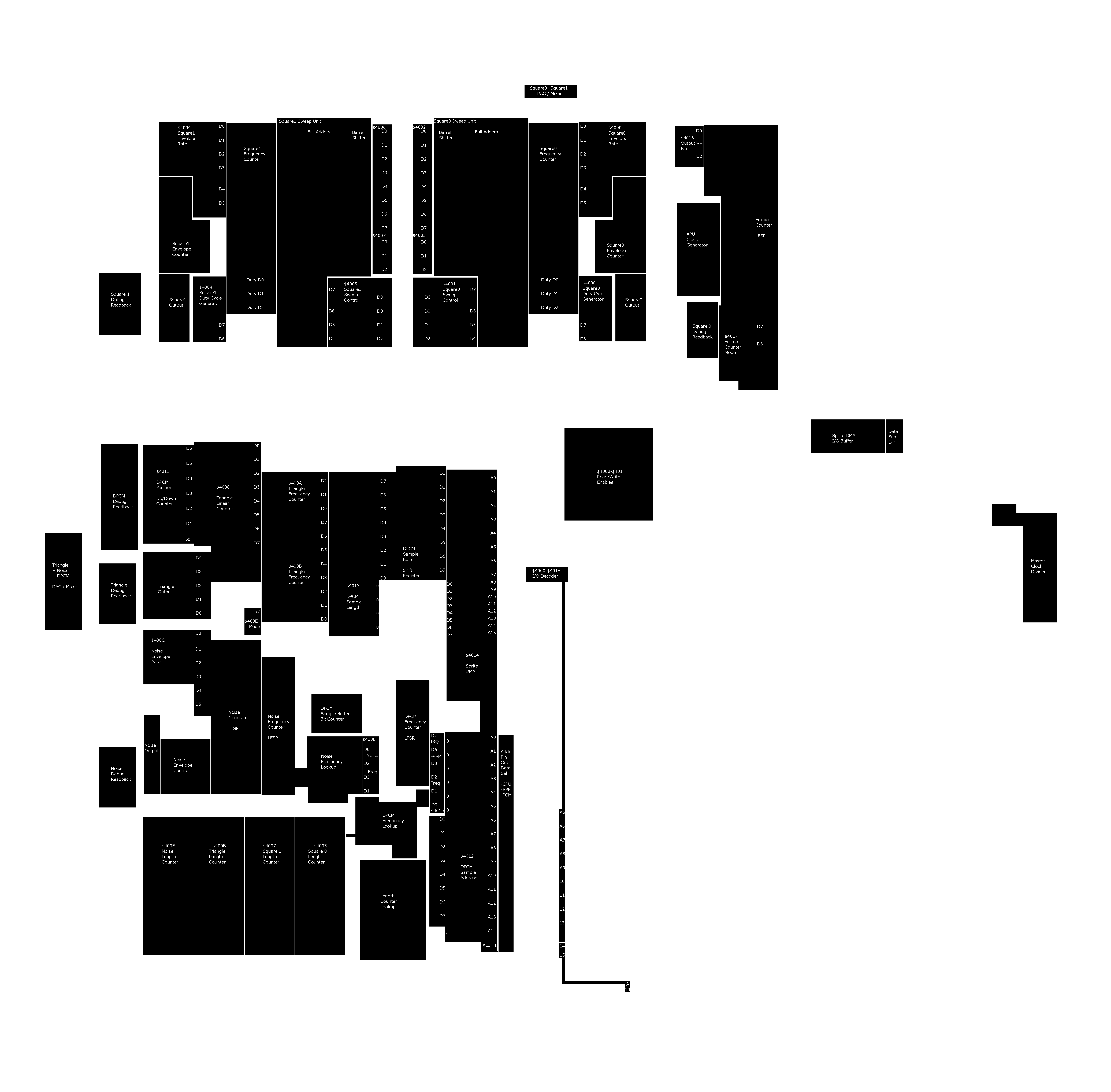
I have uploaded an overlay image for the RP2A03G which serves to label various regions of the chip according to their functionality. The image is currently incomplete, missing the two square channels - I will finish the rest of it tomorrow.
It has been a month since I last heard anything from Visual6502.org about the chip layer images I submitted, and no relevant updates have been posted anywhere on their website. Presumably, they are busy with other projects.
Based on how full adders and barrel shifters are supposed to work, the Diffusion layer image has been updated to match one possible implementation which should work unless I've gotten the logic levels backwards.
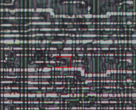
Analysis of the square channels on the RP2A03G suggests something fishy is going on - the barrel shifters and full adders* shouldn't work unless about half of the seemingly visible transistors don't actually exist, and without pictures of the die with the polysilicon layer removed I can't tell which ones exist and which ones don't (in the images I used, they all look exactly the same).
* See this image - the barrel shifter is on the left and the adders are on the right, and yellow signals are inverted from the attached blue signals. Given that each signal is steady state (the ones on the left directly correspond to register $4005 bits 0-2), only half of the polysilicon/diffusion intersections can actually form transistors.
Created yet another special page, this one being for NES-related chip images. For now, all I've got is the RP2A03G, better known as the NTSC NES CPU.
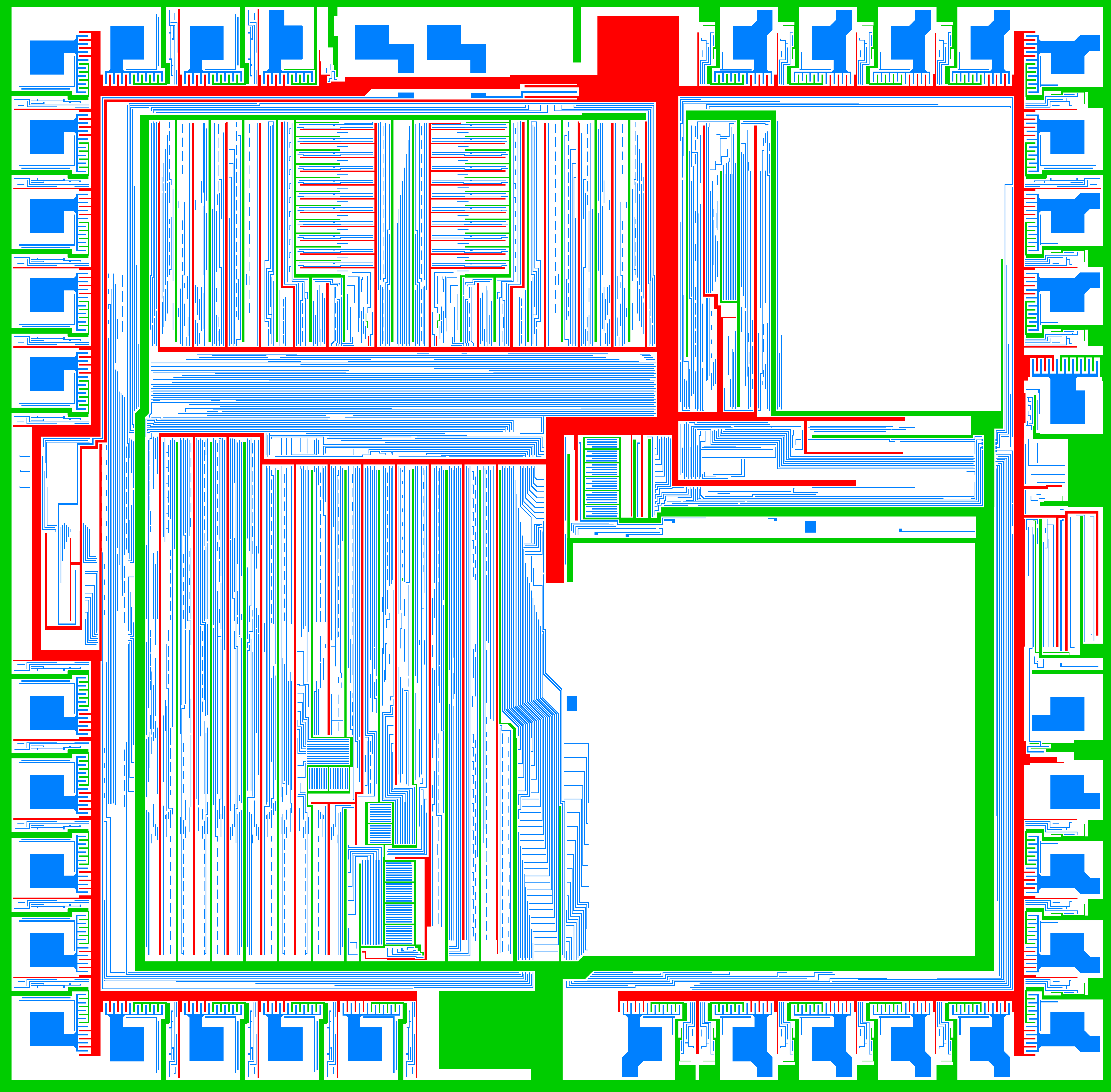
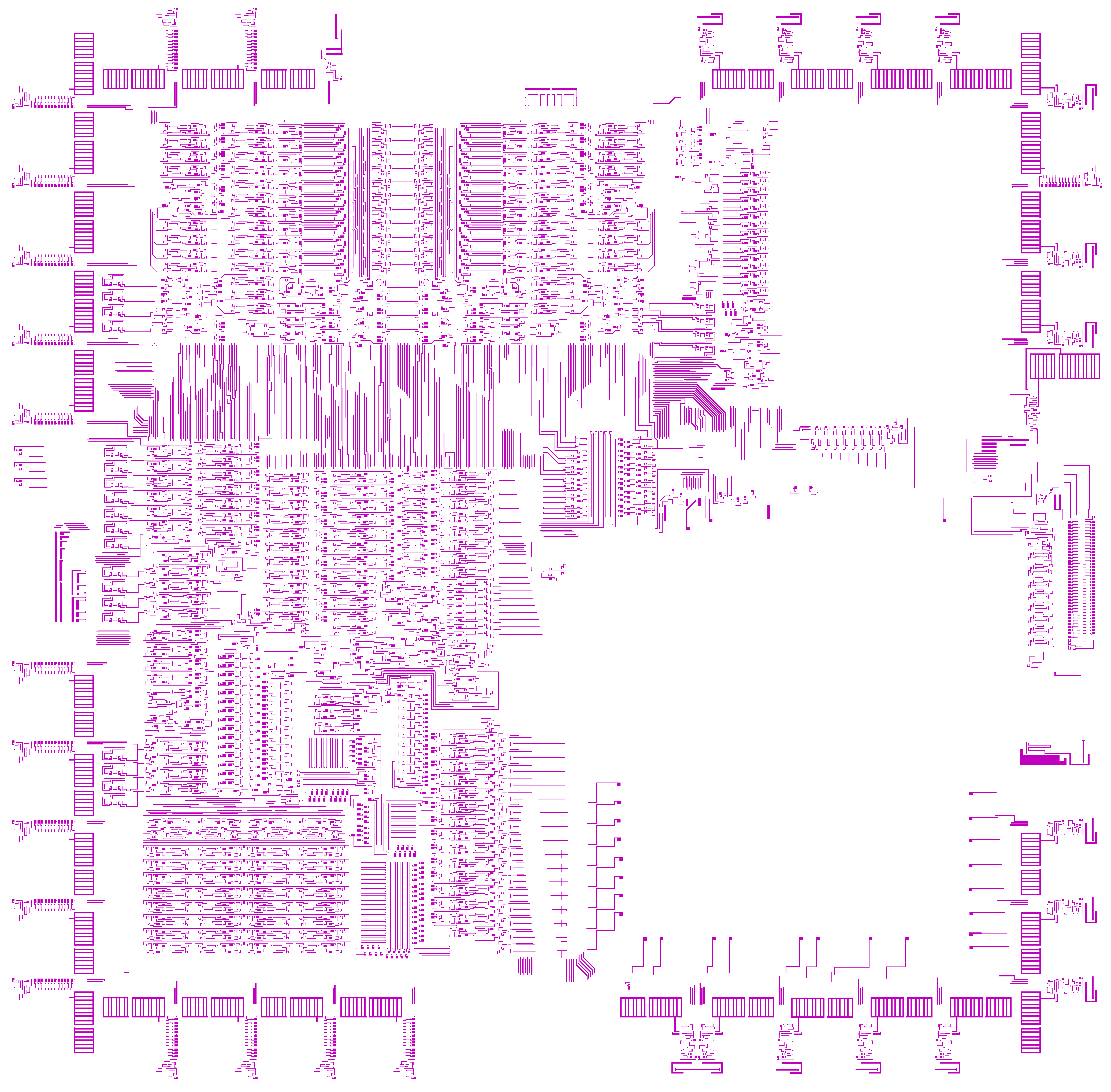
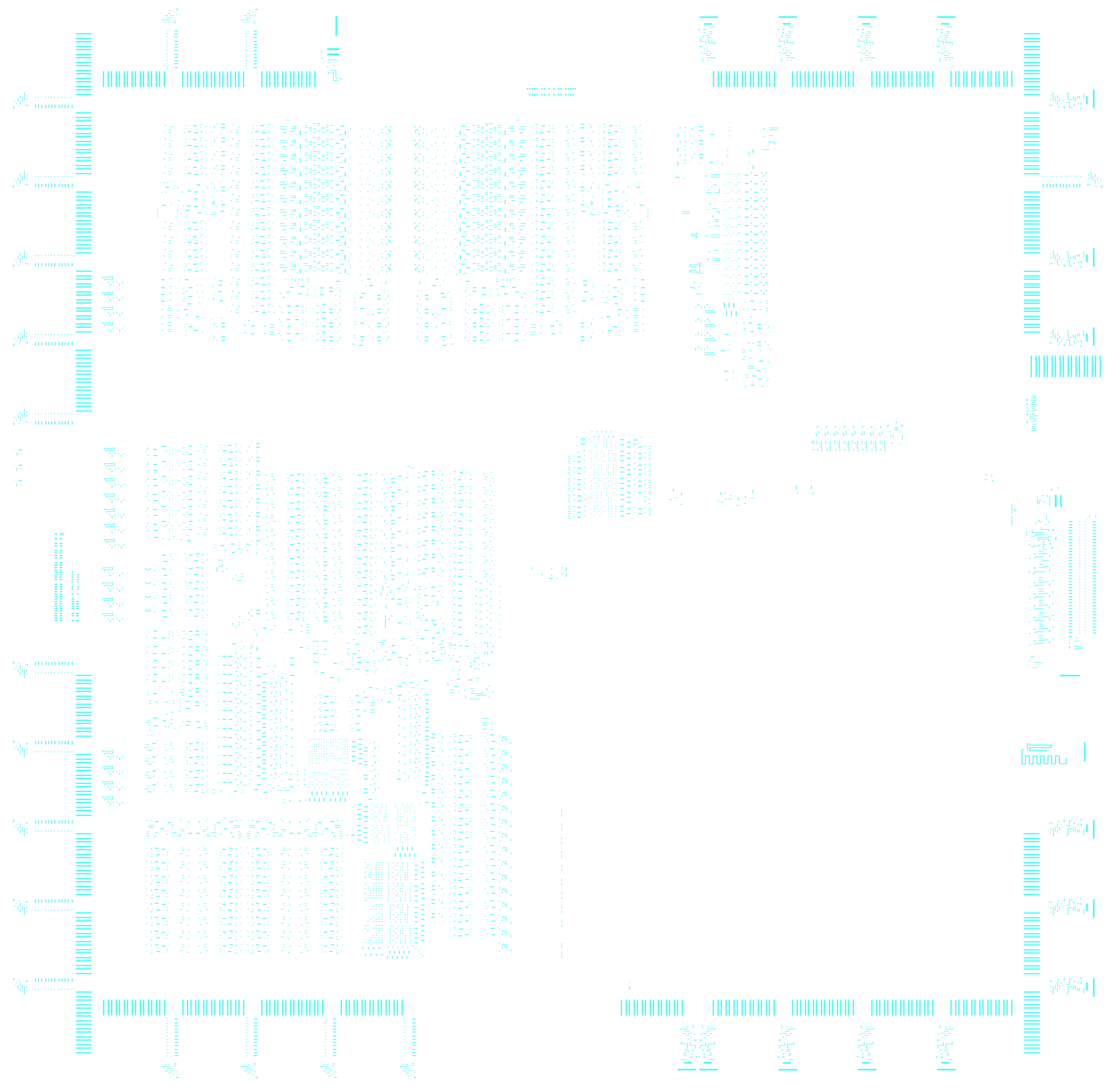
All chip images posted below are divided into several different layers. For ideal analysis, all of the images should be loaded as separate layers within a single master image using your graphics editor of choice, preferably making the Metal and Polysilicon layers partially transparent.
The layer descriptions below currently apply only to the chip images currently posted here, most of which use depletion-load NMOS logic.
- Labels
- Not an actual layer on the chip, this simply serves to assign names to various signals for reference purposes.
- Regions
- Not an actual layer on the chip, this serves to group together certain parts of the chip according to their functionality for reference purposes.
- Metal
- This layer serves to connect different parts of the chip together, though older chips also use them to form the gates of transistors (instead of polysilicon). Newer chips often use multiple metal layers in order to save space.
- In my images, red-colored metal is connected to VCC (+5V), green-colored metal is connected to GND (ground), and blue-colored metal forms interconnects.
- Vias
- Much like those found on printed circuit boards, vias form connections between layers. In this case, they connect the Metal layer to the Polysilicon and Diffusion layers.
- In my images, vias are black.
- Polysilicon
- When a Polysilicon trace passes directly between and thus connects two Diffusion regions, it forms the gate of a transistor. Polysilicon can also be used to form wires which connect sections of the chip to each other, mainly to route Metal interconnects underneath each other. In some cases, polysilicon can also be used to form capacitors and resistors.
- In my images, polysilicon traces are purple.
- Buried Contacts
- Buried Contacts are just like Vias, except they cover larger areas and are used to form direct connections between Polysilicon and Diffusion without making transistors, thus avoiding the need to jump through Vias to the Metal layer and back. Buried contacts are typically only used in NMOS chips, not CMOS.
- In my images, buried contacts are light pink.
- Transistors
- Transistors are one of the elementary components of electronics. Each transistor has 3 terminals - source, gate, and drain. The voltage applied to the gate determines the amount of resistance between the source and drain - low voltage results in high resistance (an open switch, "off"), and high voltage results in low resistance (a closed switch, "on"). The source and drain terminals of transistors are formed from the Diffusion layer, while the gate is usually made of polysilicon (though some older chips use metal gates). In depletion-load NMOS logic, certain transistors are depletion-mode - on by default, and generally used as pull-up resistors. Some chips also use depletion-mode transistors for design simplification (by allowing polysilicon to cross diffusion without forming transistors) or even to thwart reverse-engineering attempts (by creating fake transistors which don't actually do anything).
- In my images, N-type transistors are cyan and P-type transistors (only in CMOS chips and exceptionally old PMOS chips) are magenta.
- Diffusion
- Diffusion consists of conductive areas of silicon. Used alone, they can be used to form short interconnects or resistors, but their main purpose is to be used in pairs (along with Polysilicon traces running directly between them) to form the source and drain terminals of transistors. In some cases, diffusion can also be used to form capacitors and resistors.
- In my images, diffusion regions are yellow, and earlier layer images have powered regions colored orange and grounded regions colored green (while later images have them all joined together, such that the Transistors layer must first be subtracted prior to vectorizing).
Each image is also timestamped in the tables below - since I trace the individual layers manually (as opposed to using sophisticated image analysis tools), I occasionally upload new versions whenever I find errors.
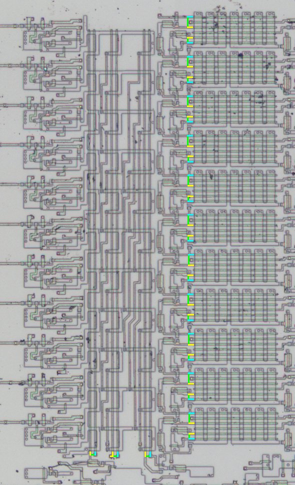
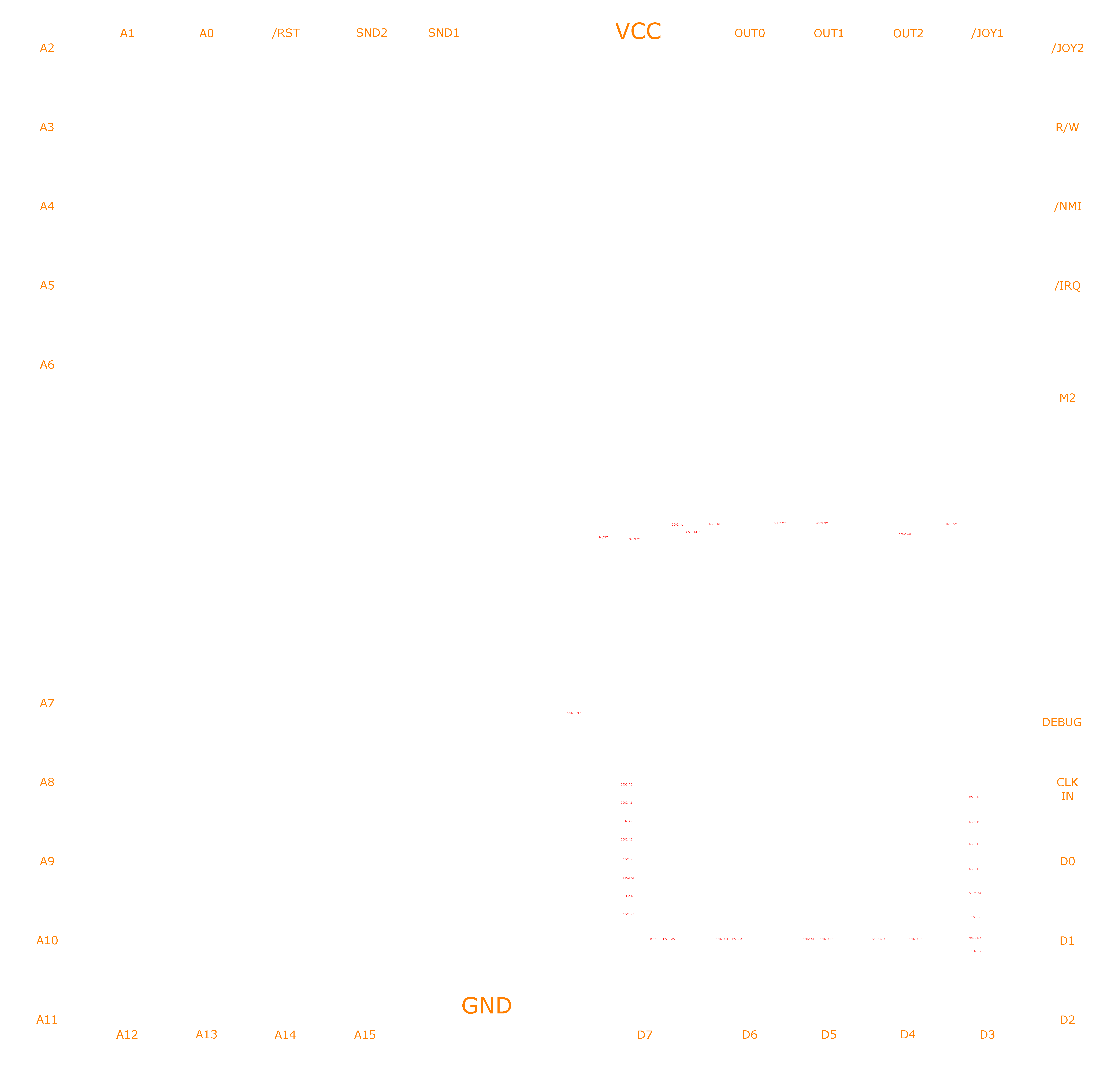
The RP2A03 is the NTSC version of the NES CPU; this particular chip is revision G. It contains 5 sound channels and a slightly modified (to remove decimal mode) MOS 6502. The 6502 itself is not included in the following layer images, mainly due to its complexity (and the fact that the Visual6502 project has already traced a real 6502).
The lack of decimal mode was seemingly intentional - 5 transistors (t1329, t2202, t2556, t2750, and t3212) were removed with surgical precision (one of which resulted in a strange "via to nowhere" observed at the very center of the following 2 images: 1, 2), the result being that the 6502's ALU no longer operates in decimal mode when the status register flag is set.
The Diffusion layer image is not 100% correct, as it was traced using the assumption that all intersections with Polysilicon formed enhancement-mode transistors (excluding the depletion-mode transistors which form pull-up resistors recognizeable both visually and programmatically). This assumption has already been proven false by the barrel shifters and full adders used in the frequency sweep logic for the 2 square wave channels - the layer image was updated to take this into account, but other similar instances may yet be lurking within the chip.
Using several special tools (and the Visual 6502 chip simulator and data), these layer images have been successfully combined to form The Visual 2A03.
Using the experience I've gathered from tracing this RP2A03, I'd eventually like to trace another one with the 6502 included, though I'll only do it if I can get better quality photographs (higher resolution, cleaner, and better focus), ideally from a fresh chip.
Errors found and fixed since making the simulator:
- Sprite DMA: 1 short (between APU clock and CPU /RDY control, prevented the 6502 from actually working)
- Square channel 0: 4 shorts (between output bits and debug readback logic)
- Square channel 1: 1 missing transistor in sweep unit high-frequency threshold detection
- Square channel 0/1 duty cycle generators: 2 bad interconnects (for duty cycle mode 01)
- Frame timer: 1 bad interconnect (in LFSR's XOR gate)
- DPCM: 4 missing transistors in timer LFSR, 1 missing via in DMA logic, 1 missing transistor in address counter, 1 missing via in length counter, 1 missing transistor elsewhere
- Noise: 1 missing via in LFSR feedback mode register
Known issues:
- The 6502 CPU was copied directly from The Visual 6502, edited to disable decimal mode, and linked to the rest of the RP2A03 using permanently-activated transistors.
- Certain parts of the chip do not function 100% correctly due to the order in which the transistors are processed in the simulator. I have attempted to fix as many of these as possible, though some may still remain.
Interesting bus names to monitor (using "Trace these too"):
- (sq0/sq1/tri/noi/pcm/frm)_(name) - registers specific to various sound channels (e.g. "sq0_len" or "tri_lc")
- envp (sq0/sq1/noi) - envelope period / volume output ($4000/$4004/$400C)
- envt (sq0/sq1/noi) - envelope timer
- envc (sq0/sq1/noi) - envelope counter (volume output)
- len (all) - length counter
- out (all) - current output bits
- p (sq0/sq1/tri) - duty cycle period ($4002-$4003, $4006-$4007, $400A-$400B)
- t (all) - duty cycle timer (noi/pcm use an LFSR)
- c (sq0/sq1/tri) - duty cycle counter (phase)
- c (noi) - random number generator (LFSR)
- swpb (sq0/sq1) - sweep bit shift count ($4001/$4005)
- swpp (sq0/sq1) - sweep period ($4001/$4005)
- swpt (sq0/sq1) - sweep timer
- lc (tri) - linear counter timer
- en (all) - channel enable (write $4015)
- t (frm) - frame timer (LFSR)
- on (all) - channel active (read $4015)
| Last Updated | Size | Layer |
|---|---|---|
| Sat, 07 May 2011 03:13:35 +0000 | 25,993 bytes | Labels |
| Wed, 08 Jun 2011 00:27:13 +0000 | 70,564 bytes | Regions |
| Thu, 23 Jun 2011 19:51:18 +0000 | 78,070 bytes | Metal |
| Tue, 05 May 2020 23:41:54 +0000 | 64,764 bytes | Vias |
| Sat, 25 Jun 2011 00:39:15 +0000 | 122,666 bytes | Polysilicon |
| Fri, 24 Jun 2011 03:45:42 +0000 | 36,056 bytes | Buried Contacts |
| Tue, 05 May 2020 18:39:38 +0000 | 54,567 bytes | Transistors |
| Wed, 27 Jul 2011 02:45:46 +0000 | 147,997 bytes | Diffusion |
The RP2C02 is the NTSC version of the NES PPU. Much of its behavior has been determined via "black box" reverse engineering, but the actual implementation of said functionality remains unknown.
The NESdev community donated several of these chips to the Visual6502 project, and several were depackaged, delayered, and photographed in order to produce the layer images below.
Several minor tweaks need to be made to these layer images for proper simulation:
- The long twisty transistor immediately to the right of the clock pin must be deleted (after subtracting it from the diffusion layer) - logically it is a resistor, and leaving it in would cause the clock pin to be ANDed with its inverse and thus not work.
- The video DAC needs to be disconnected from VCC by removing the vias immediately to the right of the clock input pin - this is simply a resistor with various taps along its length, and leaving it connected will register as a short between VCC and GND.
- Part of the sprite RAM bus precharge circuitry needs to be disconnected (specifically, the part that connects pairs of word lines to each other) by deleting the transistors from the input data - in ChipSim, minor timing glitches result in these transistors destroying the contents of sprite RAM.
- The resulting transdefs.js must be edited to reorder groups of transistors to properly simulate signal propagation direction - due to the way JSSim was written, the order in which transistors are defined affects the order in which they switch on/off, potentially resulting in incorrect simulation.
Take a look at nodenames.js for a complete list of all interesting signals to use in "Trace these too" - as with the Visual 2A03, you can specify either individual nodes or entire buses (by omitting the number from the end).
The chip simulator currently resets at the very beginning of the pre-render scanline; otherwise, writes to certain registers would have no effect until after simulating an entire frame (which takes over 30 minutes).
| Last Updated | Size | Layer |
|---|---|---|
| Thu, 11 Aug 2011 01:36:00 +0000 | 28,519 bytes | Labels |
| Sat, 14 Jul 2012 16:55:28 +0000 | 72,132 bytes | Regions |
| Sun, 14 Aug 2011 03:27:00 +0000 | 144,338 bytes | Metal |
| Sun, 18 Nov 2012 03:11:25 +0000 | 97,053 bytes | Vias |
| Wed, 19 Jun 2013 22:37:43 +0000 | 222,712 bytes | Polysilicon |
| Tue, 26 Mar 2013 00:36:29 +0000 | 43,213 bytes | Buried Contacts |
| Tue, 26 Mar 2013 00:35:25 +0000 | 126,370 bytes | Transistors |
| Wed, 31 Oct 2012 19:00:41 +0000 | 138,517 bytes | Diffusion |
The RP2A07 is the PAL version of the NES CPU. Known differences from the RP2A03 are the input clock divider (divide by 16 instead of divide by 12), assorted timer lookup values (noise, DPCM, and the frame timer), and the behavior of pin #30 (serving as a /RDY input to the 6502 rather than activating test mode registers).
The Visual6502 project claimed to have one of these chips depackaged, but no plans to delayer or photograph it were ever announced. Siliconpr0n has die shots of the topmost metal layer, but they are of poor quality and are not suitable for tracing.
The RP2C07 is the PAL version of the NES PPU. Known differences from the RP2C02 include the input clock divider, the number of scanlines per frame (and associated timing details), the generated video signal, and the sprite RAM refresh logic.
| Last Updated | Size | Layer |
|---|---|---|
| Sat, 30 Aug 2025 00:43:01 +0000 | 317,028 bytes | Metal |
| Sat, 30 Aug 2025 00:43:18 +0000 | 267,313 bytes | Vias |
| Tue, 02 Sep 2025 02:34:53 +0000 | 470,991 bytes | Polysilicon |
The 68000 is a CPU designed by Motorola, used in numerous computers including the classic Apple Macintosh and the Commodore Amiga. See Wikipedia for more information.
The layer image below was traced directly from the 10000x11299 die shots available here.
Olivier Galibert was able to produce a full transistor-level schematic of the 68000, partially assisted by this metal layer image (and some corrections).
| Last Updated | Size | Layer |
|---|---|---|
| Wed, 28 Sep 2011 00:14:06 +0000 | 291,949 bytes | Metal |
The RP2C33 is the control chip used in Nintendo's Famicom Disk System, and it is responsible for controlling the disk drive, managing interrupts, and even playing sound.
The layer image below was traced from die shots acquired from Siliconpr0n, but it is not known whether it will ever be delayered.
| Last Updated | Size | Layer |
|---|---|---|
| Sun, 15 Feb 2015 18:42:42 +0000 | 63,357 bytes | Labels |
| Mon, 22 Aug 2022 01:01:47 +0000 | 282,750 bytes | Metal |
| Mon, 22 Aug 2022 01:24:30 +0000 | 121,275 bytes | Vias |
The Konami VRC-VII is a support chip used in two Famicom game cartridges: Tiny Toon Adventures 2 and Lagrange Point.
The latter is best known for making use of the chip's expansion sound capabilities, which consists of 6-channel FM synthesis.
The chip also provides support for PRG and CHR bank switching, as well as a scanline-based interrupt counter.
The layer image below was traced from die shots acquired from Siliconpr0n, but it is not known whether it will ever be delayered.
ScottySR (who goes by the name "SCSR" on the NESdev Discord server) also independently traced all of the chip's layers (from the same source image I used); with those images (and some corrections), I was able to produce a visual chip simulator.
| Last Updated | Size | Layer |
|---|---|---|
| Fri, 19 Feb 2021 02:17:34 +0000 | 47,297 bytes | Labels |
| Fri, 19 Feb 2021 02:16:26 +0000 | 82,770 bytes | Regions |
| Fri, 19 Feb 2021 02:26:08 +0000 | 321,268 bytes | Metal |
| Fri, 19 Feb 2021 02:25:17 +0000 | 125,796 bytes | Vias |
The Nintendo MMC3 is one of the most common support chips found in NES and Famicom game cartridges.
Unlike most of the other chips featured here, the MMC3 is a CMOS chip, so ChipSim had to be modified in order to handle it properly.
This particular chip was manufactured by NEC within a 13x56 Uncommitted Logic Array (with support for up to 52 pins, of which only 44 were actually used).
The chip itself was provided to Siliconpr0n by Furrtek, traced layer images were provided by SCSR, and minor tweaks were made to fix various transcription errors.
Head over to my chipsim-tools GitHub repository for the tools I used to make the Visual 2A03. They may not be fully versatile and efficient, but they get the job done.